

Artificial Intelligence
EUV-made semiconductor chips will enable the next wave of AI

Advances in extreme ultraviolet lithography (EUV) — a technology some experts did not think would work in production just a few years ago—are transforming computer chip making. These technological gains are poised to help push today’s $600 billion global semiconductor industry to $1 trillion by the end of the decade, powering artificial intelligence (AI), high-end computing, and autonomous driving, among other advances, according to Alexander Duval, lead analyst for Europe tech hardware and semiconductors for Goldman Sachs Research.
The engineering challenges to build ever smaller, more potent, chips are enormous. Duval points out that the machines capable of creating these semiconductors cost around €300 million ($330 million) or more. The development of the latest iteration of this technology known as High NA, the next stage in the evolution of EUV, is a technology which took more than 20 years to perfect. It relies on a lens so precisely engineered that if it were expanded to the size of the Earth, the biggest blemish would be smaller than the size of a fingernail. “I’d say this isn’t rocket science; it’s harder than rocket science,” Duval says.

Alexander Duval, Goldman Sachs Research
We spoke with Duval about how this technology might be used and the extraordinary engineering challenges posed by printing ever smaller circuits onto silicon wafers.
What is EUV and how does it enable cutting-edge chip making?
There’s been an incredible evolution in this Nobel Prize-level of physics and engineering. I’d say this isn’t rocket science; it’s harder than rocket science. The technology is based on lithography, which is the process of using light to create an image of the printed circuit on a semiconductor. For about 20 years, deep ultraviolet (DUV) light has been used to create these images. The smaller the wavelength, the smaller the circuitry and the smaller the space between them, known as the pitch. In other words, shorter wavelengths lead to smaller chips. While DUV has a wavelength of 193 nanometers, EUV and High NA are 13.5 nanometers. So that’s a huge step forward.
With EUV you get high precision in terms of the printing that can be done — and that means packing more transistors into the chip and therefore the kind of processing you can do is much more powerful. High NA is the next iteration of regular EUV and utilizes a larger lens for even more granular printing needed for the most powerful chips.
What are the implications of having machines like this?
We believe EUV machines — of which High NA is the latest version — will be one the key enablers of the global semis market growing from around $600 billion today to over $1 trillion by the end of the decade. We see it as key in facilitating the production of more and more powerful chips for use cases such as AI, high-powered computing, and autonomous driving.
With AI, for example, data can be processed in real time where it’s collected, rather than sending the data to a server and waiting for an algorithm to process it and generate a response. By cutting down latency, AI can speed up decision making by several milliseconds, which can be significant for an autonomous-driving car, for example.
These new machines will build chips that are designed for edge computing, in which more powerful and energy-efficient chips are installed in devices such as automobiles, wind farms, or health care equipment. There’s a large number of interesting applications, from helping solve climate change to facilitating augmented reality.
How has your thinking evolved on EUV?
We’ve just published our latest report, a deep-dive on high NA, and we see this next-generation of extreme ultraviolet lithography (EUV) tool as the prime digital enabler. Our first report on this topic, EUV 1.0, was about whether this technology works. Our EUV 2.0 report was about how many of the first type of EUV tools (Low NA) would ship. And in our new report, EUV 3.0, we look closely at the evolution of the next generation of these machines called High NA.
What we see is a machine that is not cheap — in fact High NA tools costs €300-400 million. But it has wafer stages that accelerate with twice the G force of a rocket ship and a lens that is so precisely engineered that if it were expanded to the size of the Earth, the biggest blemish would be smaller than the size of a fingernail.
In the making of semiconductors, if you didn’t have this machine when making the most advanced chips with the smallest features, you’d be using a regular extreme ultra-violet machine and you’d have to expose the wafer many more times, something called multiple pass patterning. That has ramifications to the cost of the producer — in terms of labor and energy and time to fulfil orders.
This is a gamechanger for the semiconductor industry. When we first started out people were doubting whether the technology would work. Now we’re talking about getting 80-plus EUV machines per year by 2025, and capacity is being built for 20 High NA machines. There’s a sizeable commitment for this technology — because it works and adds a lot of value.
How close are we to seeing these machines?
We expect shipments of the first EUV machines by the end of the year, and the High NA EUV to be delivered by 2025. There’s already a double-digit number of orders for these machines — and remember we’re talking about €300-400 million per machine. When customers order the machines, they have to make down payments. That shows you the conviction these buyers have that this is something that works and has extremely important value to them. They are clearly putting their money where their mouth is.
The buyers are very sizable companies that are servicing a profitable technology ecosystem. It’s expensive per machine, but the value they are getting is very important to their business and the precision in terms of printing is very worthwhile to these buyers.
What companies are making these machines?
ASML, based in the Netherlands, is the world’s only maker of EUV machines. And there’s a whole ecosystem of suppliers and collaborators who make lasers and other modules that are vital to the EUV machine.
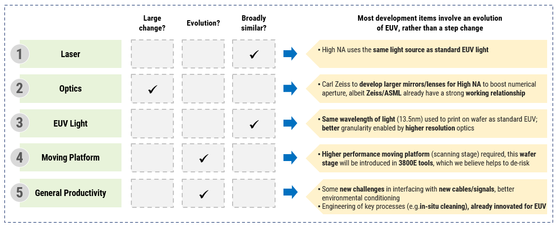
What are the execution risks for the High NA rollout?
The future High NA roadmap is meaningfully de-risked and should not face the same commercialization challenges as EUV, thereby supporting a robust level of long-term adoption. High NA will involve a new lens system, which will have a higher numerical aperture in order to achieve even more precise printing and more accurate optics, as well as faster scanning stages.
However, High NA will use several technologies that will already be used in regular low NA EUV, reducing the risk of delays and supporting a faster rate of near-term customer adoption in our view.
What’s next — what do you see on the horizon?
What we’re seeing is an evolution, rather than a revolution. There will be more to come from high NA. There’s a lot of capital in this space, a lot of innovation. When you look out to 2035 there is a clear roadmap of evolution on High NA. It’s an amazing story and pivotal in terms of the evolution of the broader tech landscape. The adoption rates of AI are yet to be understood, but AI is going to drive uses of technology. This is a meaningful part of that ecosystem.

- EUV 3.0: High NA a prime Digital Enabler for the next decade05 JUL 2023
This article is being provided for educational purposes only. The information contained in this article does not constitute a recommendation from any Goldman Sachs entity to the recipient, and Goldman Sachs is not providing any financial, economic, legal, investment, accounting, or tax advice through this article or to its recipient. Neither Goldman Sachs nor any of its affiliates makes any representation or warranty, express or implied, as to the accuracy or completeness of the statements or any information contained in this article and any liability therefore (including in respect of direct, indirect, or consequential loss or damage) is expressly disclaimed.
Subscribe to Briefings
Our weekly newsletter delivers the latest insights on economic forces shaping markets—from Goldman Sachs leaders, economists, and investors around the world.
You can unsubscribe at any time. For information about how your personal data will be used, visit Privacy Information and Resources.